eISSN: 2574-9927


Research Article Volume 2 Issue 4
New Jersey Institute of Technology, Newark, New Jersey 07102, USA
Correspondence: Ravindra NM, New Jersey Institute of Technology, Newark, New Jersey 07102, USA
Received: June 13, 2018 | Published: August 27, 2018
Citation: Bañobre A, Marthi SR, Ravindra NM. Atomic force microscopy studies of formation of black silicon by reactive ion etching. Material Sci & Eng. 2018;2(4):134-137. DOI: 10.15406/mseij.2018.02.00046
Black silicon (BSi), a surface modification of silicon, can be fabricated by various methods such as Electrochemical Etching, Metal Assisted Chemical Etching, Laser Method, etc. The fabrication of BSi by Reactive Ion Etching (RIE), under various pressures and for different etch durations, is presented in this study. The influence of pressure and etch time on the surface roughness of the resulting BSi is investigated and compared with the literature.
Black Silicon (BSi), a surface modification of silicon, is being used in a variety of applications including image sensors, bio–sensors, Micro–Electro Mechanical Structures (MEMS), light–emitting devices, anti–reflection coatings and antibacterial coatings.1–4 The unusually low reflectance and high absorptance of BSi make it an attractive candidate in silicon solar cell technology.5–8 Several methods have been used to process BSi. These methods include the following: Metal Assisted Chemical Etching,9–16 Electrochemical Etching17–19 and Laser Method.19–27 Non–conventional etching techniques may be hazardous, complex and not easily scalable.28
In the present study, we utilize the conventional Reactive Ion Etching (RIE) method for the processing of BSi. The formation of BSi structures with varying etch conditions is presented. An Oxford PlasmaPro NGP0 RIE system is utilized in these experiments. The Oxford PlasmaPro NPG80 RIE is an open–load medium plasma density system configured for fluorine–based etch chemistries, which can accommodate pieces to wafers up to 8” in diameter and 3 cm thick. The rate of flow of gases, SF6, O2 and CHF3, is fixed. The chamber pressure and etch time have been varied to study the surface structure formation.
Reactive ion etching
The use of RIE for the formation of grass like BSi structures was first reported by Jansen et al. around 1995.29,30 The RIE system consists of two parallel–plate electrodes. One wafer may be loaded onto the bottom electrode, called the cold cathode, for each run. A high vacuum is formed using a turbomolecular pump. The gases are supplied from the edge of the upper electrode.31 The RIE process can provide high rates of isotropic etching, which makes it possible to vary the etch directionality between isotropic and anisotropic etching using SF6/O2 at various flow rates.32 In SF6/O2/CHF3 plasma, each gas has its specific function and influence. The etch profile may be controlled by varying the flow rates of the gases.
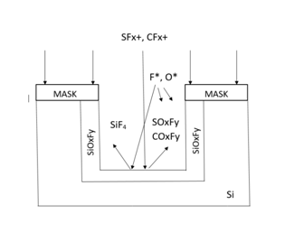
SF6 produces F* radicals for the chemical etching of silicon by forming volatile SiF4. O2 creates O* radicals to passivate the surface of Si wafer with SiOxFy. SFx radicals remove the oxyflouride. The CHF3 gas is almost an independent source of oxyflouride etch ions.
These gases are responsible for the highly controllable profiles at very low ion energies and also high etch rates. The low ion energy prevents substrate damage, and makes it easy to change the profile of the trench. The ion energy is governed by the potential which is developed between the plasma and the powered electrode, the DC self–bias. Gases such as O2 and CHF3 are used at high bias voltages, whereas SF6 requires very low voltage. The SF6/O2/CHF3 etching mechanism is shown in Figure 1.

Figure 1 1The SF6/O2/CHF3 chemistry {based on Figure from}.29
Experimental details
In the present study, single side polished p–type <100> CZ wafers with substrate resistivity of 0.010–0.020 Ω–cm, 5–inch diameter and 600 μm thickness are used. The wafers are cut to 1 square inch samples after standard cleaning. SF6, O2 and CHF3 gases are used for the etching process with flow rates of 33 sccm, 11 sccm and 13 sccm respectively. Chamber pressures are varied from 60 mTorr to 100 mTorr. The plasma power is maintained at 100 W for all the etching processes. Various conditions of etching, implemented in this study, are summarized in Table 1. Fifteen to Twenty samples were prepared for each process run. Out of these, five were used for AFM measurements. The AFM results, presented in this study, represent a characteristic image for each process. Average of the results of roughness has been presented in Table 2. A Bruker Atomic Force Microscope, Model – Dimension FastScan, has been utilized in acquiring the AFM images.
Sample |
Pressure (mTorr) |
Etch time (minutes) |
Sample A |
100 |
10 |
Sample B |
100 |
20 |
Sample C |
100 |
30 |
Sample D |
80 |
10 |
Sample E |
60 |
10 |
Sample F |
60 |
15 |
Table 1 Summary of etch conditions used in the present study
Sample |
Roughness (nm) |
Structure profile |
Sample A |
20.4 |
Columnar |
Sample B |
29.1 |
Pyramidal |
Sample C |
11 |
Non-uniform pyramids |
Sample D |
69 |
Columnar |
Sample E |
45.9 |
Pyramidal |
Sample F |
51.1 |
Pyramidal |
Table 2 Summary of roughness and structure profile
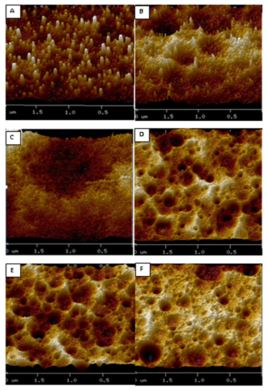
AFM images of six samples, processed in this study, are presented in Figure 2. This figure shows the distribution of varying surface roughness for the samples. It may be observed that, at higher pressures, the trenches are wider than that at lower pressures. The roughness varies between 11 nm to 69 nm. The 3D view of the AFM image, showing the roughness, is presented in Figure 3.

Figure 2 Top view of Samples A-F. The corresponding viewing areas of samples, imaged under the AFM, are 4 μm2.

Figure 3 3D view of Samples A-F. The corresponding viewing areas of samples, imaged under the AFM, are 4 μm2.
At a pressure of 100 mTorr, for 10 minute etch duration (sample A), the resulting structures are columnar structures of roughness 20.4 nm. For higher etch durations, viz., 20 minutes and 30 minutes, the structures are pyramidal and non–uniform pyramidal structures with roughness of 29.1 nm and 11 nm respectively. Further, at 80 mTorr, for 10 minute etch duration, the structures formed are columnar. The roughness of the sample is about 69 nm. With further decrease in chamber pressure, at 60 mTorr, 10 minute etch results in pyramidal structures with roughness of 45.9 nm. At the same pressure, for longer etch time of 15 minutes; the resulting structures are pyramidal with roughness of ~51 nm.
For higher pressures, i.e. 100 mTorr in these experiments, the surface of the silicon sample consists of holes of increasing diameter throughout its surface area. Increase in pressure and etch time leads to increase in the recombination of F* radicals. Since all the processes have similar gas flow rates, the uncombined F* and O* radicals have increased times to react with the silicon as the etch times increase. However, for etch times greater than 20 minutes, the holes formed are larger and the roughness of the surface is decreased as the higher pressure reduces the energy of the delivered ions.
The roughness is observed to be maximum for a pressure of 80 mTorr for etch time of ten minutes. The summary of roughness and structure of the resulting profile is summarized in Table 2.
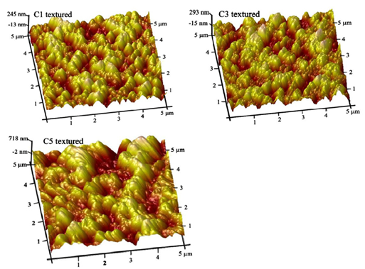
Figure 4 shows the AFM images of microstructures of black silicon wafers with different texturing conditions. Zhong et al.,33 have utilized Plasma Immersion Ion Implantation method33 for processing black silicon. Figure 4 shows that the black silicon surfaces are covered with dense nano hillocks, and the roughnesses of the nano hillocks are 150 nm, 300 nm and 600 nm for the surfaces of the C1 textured, C3 textured and C5 textured, respectively.

Figure 4 AFM images of microstructures of black silicon wafers with different texturing conditions.33
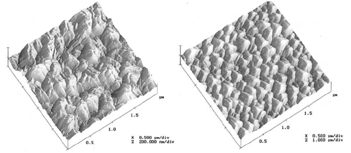
Figure 5 shows AFM surface scans obtained by Dekkers et al.,34 for different RIE etching conditions. The profile of the resulting BSi structure in both the studies is pyramidal. The structure and roughness of BSi obtained by various research groups, in the literature, is tabulated and is compared with the present study in Table 3. The difference in the size of roughness of BSi structures is due to the difference in the rate of flow of gases and difference in applied chamber pressure.

Figure 5 AFM surface scans, obtained by different RIE conditions.3
Study |
Roughness |
Process |
Structure profile |
Present Study |
69.0 nm* |
RIE |
Columnar |
Zhong et al. 33 |
600 nm |
PIII |
Nano hillocks |
Mazur et al.21 |
40 μm |
Laser |
Spikes |
Su et al.4 |
470 nm |
Wet Etching |
Micro-columns |
Table 3 Comparison of structure profile and roughness of BSi
*best obtained
Reactive Ion Etching (RIE) has been utilized to form BSi with varying morphologies. RIE can produce nano needles of silicon of varying heights and very low reflectance (less than 5%) can be achieved. RIE is the most suitable process for obtaining low reflectance and is also cost effective. The change in the surface morphology, as function of process parameters, has been studied. The influence of pressure and etch time on the surface roughness and structure profile has been examined. The obtained roughness is compared with the study in the literature.
We thank Dr. Michael Ehlrich and Ms. Judith Sheft of NJIT/NJII, for providing partial funding for the project through NSF–I–Corps towards the processing of the wafers. This work has been performed in part at the Advanced Science Research Center (ASRC) Nano Fabrication Facility of the Graduate Center at the City University of New York (CUNY). We thank Dr. Vishal Narang and Dr. Jacob Trevino for helping us with materials processing.

©2018 Bañobre, et al. This is an open access article distributed under the terms of the, which permits unrestricted use, distribution, and build upon your work non-commercially.